

UnitySC is a worldwide leader in Semiconductor Metrology & Inspection solutions
Let’s explore UnitySC
WE ENABLE OUR CUSTOMERS TO YIELD HIGHER & FASTER

WHO ARE UNITYSC?
UnitySC was formed in 2016, by a combination of European companies. Headquarted in France, UnitySC has a worldwide footprint, with staff in every major chip producing region.

WHAT DOES UNITYSC MAKE?
UnitySC is a leader in creating Metrology & Inspection tools used for Advanced Packaging (TSVs, High BandWidth Memory Chip stacks, Hybrid-Bonding/Wafer2Wafer, Die2Wafer) & MEM’s.
We also make equipment for unpatterend wafer defect inspection (all types of Compound-semi substrates like GaN, GaAs, InP, SiC, Glass, Sapphire, Ge, Silicon).
Plus other Metrology & Inspection equipment for other use-cases, all of which are used by our customers for yield improvement.

WORKING AT UNITYSC
At UnitySC, we promote and support from a diverse talent pool. We are pushing the frontiers of technology, making us an attractive place to work that allows all our employees to grow and succeed.

UNITYSC’S SERVICES
UnitySC are able to offer resources for Service & Applications Support for our equipment to customers all over the world.
We provide a comprehensive range of maintenance, upgrade and other services, depending on your requirements. Through these services, we can continuously maintain the health of your tools over their lifetimes.
Our Spare Parts Team offers a quick and reliable service to keep your production lines moving.
EXAMPLES OF OUR CUSTOMERS’ END MARKETS
Automotive
The move from ICE vehicles to E-vehicles, Autonomous driving (eg; ADAS), in-car-tech, digital connectivity & security. All these trends have one common enabler: Semiconductor components.

High-Bandwidth Memory (HBM)
High-Performance Computing (HPC)
AI-driven data analytics require real-time data processing at scale. UnitySC optimizes Semiconductor industry computing and memory architectures (GPU & CPU) for efficient handling of large and time-critical datasets.
Enhancing overall performance in data analytics, more efficiently and securely handled.

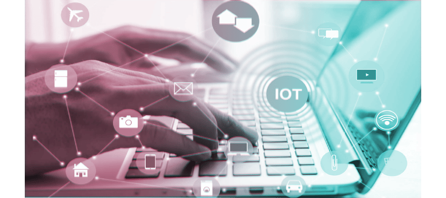
Internet Of Things
IoT technology in its ultimate form will consist of an ecosystem of securely hyperconnected devices driving the world of tomorrow. In short, more & more physical products will contain more & more chips of all types of functions.
AI & Augmented
Virtual Reality
Augmented reality and artificial intelligence are distinct technologies, but together they create unique digital experiences.
These technologies require smaller form factors, higher performance chip-materials and novel packaging approaches.

What’s new
Press releases
Léa ALZINGRE, CFO of Soitec, joins UnitySC board of directors
UnitySC is delighted to announce the appointment of Léa ALZINGRE, CFO of Soitec, as an independent member of its board of directors and chairwoman of the audit committee. Her history Léa ALZINGRE has been CFO of Soitec since July 2020. Soitec (Euronext Paris)...
Paul Boudre appointed chairman of UnitySC
UnitySC, a leading provider of metrology and inspection equipment for the semiconductor industry, is delighted to announce the appointment of Paul Boudre, former CEO of Soitec, as chairman of its board of directors. Paul Boudre was the CEO of Soitec [EPA:SOI], a world...
Events
Join UnitySC at SEMICON EUROPA 2023, Booth 701, Hall B0: A Gateway to Semiconductor Innovation
Mark your calendars for November 14-17, 2023, as Munich gears up to host SEMICON EUROPA, a pivotal event in the world of semiconductors. If you're in the industry, this is an opportunity you simply can't afford to miss. The UnitySC European team is thrilled to...
Join the UNITY-SC team at SEMICON EUROPA from November 15-18, 2022 in Munich, a key meeting for the semiconductor market.
UnitySC European team will be pleased to welcome you at booth 160, hall C1, in Messe München, Munich, Germany. Visit us to discover our range of inspection and metrology tools combining advanced technologies used for Unpatterned & Patterned Defect...
News
Romain: Bridging Software Excellence and Employee Advocacy at UnitySC
Romain brings a wealth of knowledge to UnitySC, with an educational background in System Integration Engineering, essential skills in computer science, and a specialization in Image and Signal Processing. Since joining UnitySC in 2012, Romain has leveraged his...
UnitySC rejoint France Deeptech en novembre 2023, la communauté qui rassemble les acteurs de la deeptech pour une réponse entrepreneuriale, collective et scientifique à nos défis contemporains
UnitySC est désormais membre officiel de France Deeptech, une association révolutionnaire lancée officiellement le 29 novembre à la BnF Richelieu, sous le patronage distingué de trois ministres éminents – Sylvie Retailleau, Roland Lescure et Jean-Noël Barrot. Ce...